![]()
In the wave of continuous miniaturization and performance improvement of electronic products, high-density interconnect (HDI) PCB design has become the standard. This poses a serious challenge to traditional identification technologies used for asset tracking: extremely limited space and the need for higher reliability. The ultra-micro UHF RFID tag, with a size of only 2.6mm, has emerged to address this challenge. It is not simply a miniaturized chip, but a complete embedded tag system solution that can be directly integrated into PCBA packaging.
In-Depth Technical Analysis: A Complete Tag Solution Beyond the Chip
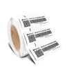
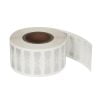
When we discuss 2.6mm RFID, we are usually referring to a complete package containing the RFID chip and a miniaturized antenna. Its core is flip-chip or wafer-level chip-scale packaging (WLCSP) technology, combining microchips such as Impinj Monza R6, NXP UCODE 9, or Alien Higgs-9 with custom antennas, packaged into a component suitable for SMT (Surface Mount Technology).
This tag complies with the EPC Gen2v2 / ISO/IEC 18000-63 standard and operates in the 860-960MHz frequency band, achieving a stable reading distance of 0.3 meters to 1.2 meters in typical application environments (such as SMT production lines or near test fixtures).
Four Core Values in High-Density PCBA Packaging
- Extreme Space Compatibility: The tag can be placed on the edge of the PCB, under the heat sink, or even integrated into the flexible area of a rigid-flex board. Its small size avoids layout conflicts with high-speed signal lines (such as DDR or PCIe) and BGA packages, forming the basis for achieving high-density tracking without affecting electrical performance.
- Process Automation and Process Robustness: As a standard SMT component, it can be placed with high speed and precision alongside resistors and capacitors using a pick-and-place machine, and withstand standard lead-free reflow soldering temperature profiles (peak approximately 260°C). This eliminates subsequent manual labeling steps, and the label is integrated with the PCB, making it wear-resistant and corrosion-resistant.
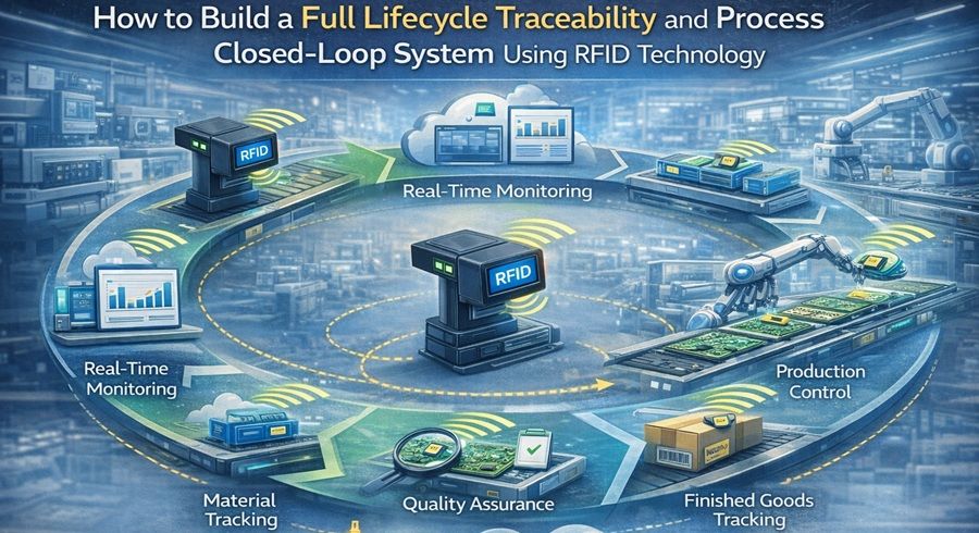
- Full Lifecycle Data Carrier: The label becomes part of the board’s identity from the solder paste printing stage, and can be used throughout in-circuit testing (ICT), functional testing (FCT), assembly, logistics, and after-sales service, providing a physical data anchor point for building digital twins and achieving product lifecycle management (PLM).
- Enhanced Security and Configuration Management: The chip memory can be partitioned to store unique serial numbers, calibration data, security keys, or version information, enabling hardware-level anti-counterfeiting, tamper-proofing, and on-site configuration verification.
Solution Comparison: Ultra-Miniature Embedded Tags vs. Traditional Identification Methods
| Comparison Dimension | Screen Printing/QR Code | External RFID Tag | 2.6mm Embedded RFID Tag |
| Physical Size | Occupies large planar space | Usually > 4mm x 4mm | Extremely small (~2.6mm), space-efficient |
| Integration Process | Printing, possibly completed in post-processing | Manual or semi-automatic attachment, later in the process | Fully automatic SMT placement, integrated in the early stages of the process |
| Environmental Durability | Easily corroded by chemicals and physically worn | Adhesive may age and peel off | Welded and fixed, resistant to high temperatures, chemical cleaning, and vibration |
| Data Readability | Requires optical line of sight, read individually | Non-line of sight, batch reading | Non-line of sight, batch reading, strong anti-interference |
| Data Capacity and Security | None | Read/write, medium to large capacity | Read/write, large capacity, supports encrypted partitions |
| Overall Cost | Lowest (single instance) | Medium | Higher, but total cost of ownership (TCO) is reduced due to increased efficiency |
Key Engineering Practice: RFIDHY’s Customized Antenna and Integration Services
Successfully applying 2.6mm RFID tags to diverse PCBA designs, the core challenge lies in antenna design. The performance of the trace antenna on the PCB is greatly affected by the substrate material (such as FR-4, Rogers), stacking structure, surrounding ground plane, and component layout. RFIDHY’s core strength lies in providing deeply customized collaborative design services:
- Antenna Simulation and Optimization: Utilizing professional electromagnetic simulation software, we custom-design optimal on-board antennas based on the customer’s specific PCB layout, ensuring reliable reading in complex electromagnetic environments.
- Material and Process Package Support: We provide a complete process documentation package, including stencil design recommendations, solder paste recommendations, and reflow soldering curve guidance, ensuring successful label integration in the SMT process.
- System-Level Debugging and Verification: We assist in deploying and debugging fixed or handheld readers (such as RFIDHY HY-R6100 or HY-R346A) in the customer’s actual production environment, optimizing reading strategies to achieve a reading rate of over 99.9%.
Q&A
1.Will integrating an RFID antenna on a PCB filled with high-frequency digital signals and RF circuits cause interference?
With professional design, interference can be minimized. The key lies in careful frequency band planning and layout isolation. RFID antennas are typically designed at specific frequencies (such as 915MHz), and utilize ground shielding and maintaining a safe distance from critical signal lines (such as clock lines and RF traces) to avoid coupling. RFIDHY’s engineering services include such critical electromagnetic compatibility (EMC) co-simulation to ensure the label works harmoniously with the main circuit.
2.Is this embedded label solution suitable for small-batch, multi-variety R&D or pilot production stages?
Absolutely, and it brings significant value. Even in small-batch production, tracking test data, configuration changes, and transfer history for each prototype board is crucial. RFIDHY provides standard evaluation kits and flexible design services suitable for small batches, helping R&D teams quickly verify the integrated solution and pave the way for mass production.
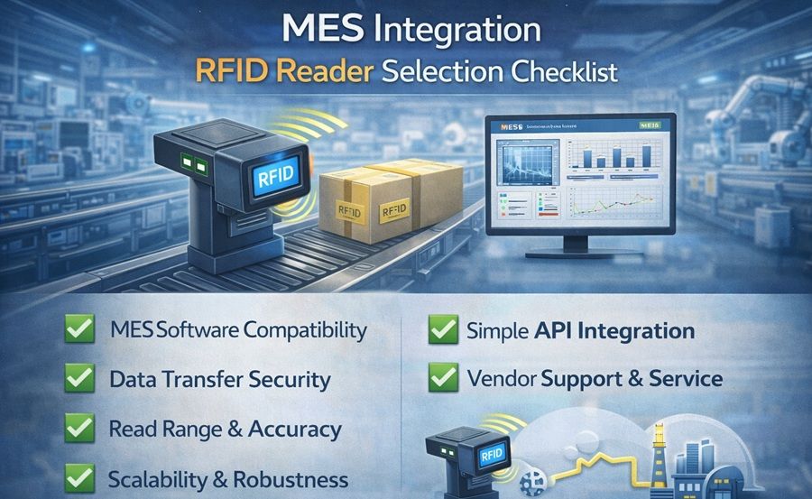
3.How can the label data be integrated with the factory’s MES or ERP system, and cloud platform?
This is a standard integration process. After the RFID reader on the production line captures the tag’s EPC code, it is processed by an edge computing device or RFID middleware (such as RFIDHY FabVis). The event data, including “when, where, and which board,” is then pushed in real-time to the Manufacturing Execution System (MES), Enterprise Resource Planning (ERP), or cloud-based IoT platform via standard protocols such as RESTful API, MQTT, or OPC UA, enabling data-driven decision-making.
Conclusion
The 2.6mm ultra-micro RFID tag has surpassed the traditional concept of “identification,” becoming a fundamental component enabling high-density, intelligent electronic products. It directly embeds high-density tracking capabilities into the core of PCBA packaging, providing irreplaceable value in improving manufacturing efficiency, ensuring product quality, and optimizing supply chain management through automated data collection throughout the entire process.
Collaborating with experts like RFIDHY, who possess deep expertise in customized antenna design and system integration, is crucial for the rapid and reliable implementation of this cutting-edge technology and unlocking its full business potential.
Leave your contact detail now to get the latest price!