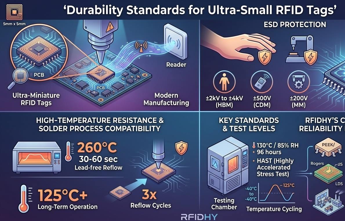
1.What Are Ultra-Small RFID Tags?
Ultra-Small RFID tags refer to tiny tags typically measuring 5mm × 5mm or less—some as small as 2.6mm × 2.6mm. They typically employ Flip Chip or Wafer-Level Chip-Scale Package (WLCSP) technologies to integrate a UHF RFID chip (such as the Impinj Monza R6 or NXP UCODE 9) with a miniature antenna, forming a standardized component that can be directly mounted using Surface Mount Technology (SMT).
In modern high-tech manufacturing—particularly within SMT production lines, semiconductor packaging, and automotive electronics—ultra small RFID tags face challenges far beyond simple readability. They must withstand a gauntlet of multiple stresses, including Electrostatic Discharge (ESD), extreme temperatures, and chemical corrosion. A clear and comprehensive white paper on reliability standards serves as the cornerstone for ensuring that these high-temperature-resistant tags operate stably in harsh environments while remaining perfectly compatible with existing soldering processes.
2.ESD Protection: Safeguarding Sensitive Chips and Data
Static electricity is ubiquitous, especially within dry cleanroom environments. Even a minor ESD event can result in logic errors within the RFID chip, memory corruption, or even permanent device failure. To address the ESD protection requirements of ultra small RFID tags, the industry has established rigorous testing standards:
- Human Body Model (HBM) Testing: Simulates electrostatic discharge from the human body. In accordance with the ANSI/ESDA/JEDEC JS-001 standard, industrial-grade ultra small tags are typically required to pass test levels of ±2kV (Class 2) or ±4kV.
- Charged Device Model (CDM) Testing: Simulates the discharge that occurs when a device itself has accumulated a static charge; required tolerance levels typically reach ±500V or higher.
- Machine Model (MM) Testing: Simulates contact discharge from automated equipment; typically requires a tolerance capability of ±200V.
For instance, the Impinj Monza R6-P chip boasts an HBM ESD tolerance of up to ±4kV—far exceeding standard industry requirements. Similarly, the NXP UCODE 9 series features excellent on-chip ESD protection circuitry. Selecting high-temperature-resistant labels featuring chip packages that meet these reliability standards constitutes the primary step in mitigating ESD risks at the source.
3.High-Temperature Resistance and Solder Process Compatibility—Harmonizing with PCBs
For ultra small RFID tags that require direct embedding into a PCBA or must endure high-temperature stages within a production line, compatibility with soldering processes is of paramount importance. This compatibility is primarily demonstrated through the following criteria:
- Reflow Soldering Tolerance: The label must be capable of withstanding the temperature profiles associated with lead-free reflow soldering. In accordance with the JEDEC J-STD-020 standard, this typically requires enduring a peak temperature of 260°C for a duration of 30 to 60 seconds, and successfully surviving three or more reflow cycles without any degradation in performance.
- Long-Term Operating Temperature: In environments involving automotive electronics or proximity to high-power devices, the label must be capable of sustained operation within high-temperature settings—specifically at 125°C or even higher.
- High Accelerated Stress Test (HAST): In accordance with the JESD22-A110 standard, this test involves applying a bias voltage for 96 hours within an extreme environment of 130°C and 85% relative humidity (RH) to evaluate the packaging material’s resistance to moisture and corrosion.
- Temperature Cycling Test: The label undergoes hundreds of thermal cycles ranging from -40°C to 125°C to simulate and assess the impact of thermal stress under actual operating conditions.
4.Key Standards and Test Level Comparison Table
| Robustness Dimension | Relevant International Standard | Typical Test Levels/Requirements | Representative Passing Chips/Packages |
| ESD Protection (HBM) | ANSI/ESDA/JEDEC JS-001 | ±2kV (Class 2) to ±4kV | Impinj Monza R6 Series, NXP UCODE 9 |
| ESD Protection (CDM) | ANSI/ESDA/JEDEC JESD22-C101 | ±500V | Alien Higgs-9 |
| Reflow Peak Temperature | JEDEC J-STD-020 | 260°C (Lead-free), >3 cycles | RFIDHY HT Series Encapsulated Tags |
| High-Temperature Storage | MIL-STD-883 Method 1008 | 150°C, 1000 hours | Industrial tags utilizing PEEK or ceramic encapsulation |
| High-Temperature, High-Humidity Bias | JESD22-A110 (HAST) | 130°C / 85% RH, 96 hours | RFIDHY Industrial-Grade Encapsulation |
| Temperature Cycling | JEDEC JESD22-A104 | -40°C to 125°C, 500 cycles | Specialized Wafer-Level Encapsulated Tags |
5.Beyond the Standards: RFIDHY’s Customized Reliability Engineering
Standards serve as the foundation; however, the true challenge lies in the “non-standard” rigors of specific production line environments. Examples include thermal shock from the side during wave soldering, ion bombardment during plasma cleaning processes, or chemical corrosion from plating solutions. This is precisely where RFIDHY’s core value lies:
- Customized Encapsulation Design:For scenarios requiring resistance to extreme temperatures exceeding 260°C (such as certain power module sintering processes), we provide customized encapsulation solutions utilizing ceramic substrates and gold wire bonding. For environments involving chemical corrosion, we offer specialized encapsulation materials such as perfluoroether rubber or PEEK.
- Embedded Antenna Material Optimization:To address signal attenuation issues at specific frequencies, we utilize Rogers high-frequency laminates as the antenna substrate or employ LDS (Laser Direct Structuring) technology to directly form antennas on 3D surfaces, ensuring stable RF performance is maintained even under high-temperature conditions.
- End-to-End Reliability Verification:We provide comprehensive engineering services—ranging from chip selection and antenna simulation to sample HAST (Highly Accelerated Stress Test) and thermal cycling verification—to ensure that every tag meets long-term reliability standards within the customer’s specific manufacturing processes.
- On-Site Environmental Simulation Testing:We collect actual process parameters directly from the customer’s production site, then replicate these conditions in our laboratory to establish an environmental simulation platform, thereby verifying the long-term stability of the tags under real-world operating conditions.
Q&A
Q1: What is the biggest difference between ultra small RFID tags and traditional tags?
A:The primary difference lies in their integration methods and application scenarios. Traditional RFID tags are typically external, surface-mounted devices with larger dimensions, making them suitable for attachment to product packaging or the surfaces of large assets. In contrast, ultra small RFID tags are designed to be directly embedded *inside* PCBs, semiconductor carriers, or minimally invasive surgical instruments. They can be automatically mounted via SMT processes, becoming an integral part of the product itself, thereby enabling true component-level tracking and embedded identity authentication.
Q2: How can I determine if a “high-temperature-resistant tag” is truly suitable for my specific reflow soldering process?
A:You cannot rely solely on the nominal temperature rating. You must verify whether the tag has successfully passed JEDEC J-STD-020 level testing—specifically the level corresponding to your process requirements—and confirm its “Moisture Sensitivity Level (MSL).” Additionally, you should request that the supplier provide data on the RF performance degradation (e.g., changes in reading distance) of their tags after undergoing multiple reflow cycles. Professional suppliers like RFIDHY will provide detailed test reports rather than merely offering theoretical values.
Q3: Does ESD protection mean that an RFID tag can be handled freely in any environment without concern?
A:An ESD protection rating (e.g., HBM ±2kV) indicates the tag’s tolerance under controlled test models; it does not imply that one can disregard all sources of static electricity. In actual operations, it is still necessary to adhere to basic ESD safety protocols (such as wearing grounded wrist straps and using anti-static packaging). However, a high protection rating significantly reduces the probability of accidental damage, thereby improving manufacturing yield rates.
Q4: How is the read performance of ultra small RFID tags guaranteed in metal environments?
A: Metal environments can severely interfere with RF signals. Beyond considerations for temperature resistance and ESD protection, the core challenge lies in antenna design. In such cases, specialized, custom-designed “anti-metal” tags are required; these tags utilize ceramic antennas, magnetic dielectric substrates, or specialized magnetic field coupling techniques to leverage the metal surface as a reflector—effectively transforming a potential “disadvantage” into an asset that enhances signal strength. RFIDHY possesses extensive experience in custom solutions within this field and can design optimized strategies tailored to a client’s specific metal environment.
Q5: What special considerations apply to ultra small RFID tags that need to be embedded within plastic or ceramic packaging?
A: When tags are embedded within non-metallic materials, the material’s dielectric constant (Dk) and dielectric loss (Df) can impact the antenna’s resonant frequency and radiation efficiency. This necessitates precise modeling and tuning during the design phase, typically achieved through the use of electromagnetic simulation software. RFIDHY offers comprehensive co-design services, assisting clients in integrating the RFID tag’s antenna characteristics into the packaging design process from the very outset, thereby ensuring optimal read performance for the final product.
Leave your contact detail now to get the latest price!