In highly automated wafer manufacturing environments, the accurate tracking of FOUPs and SMIF Pods directly impacts productivity, yield, and operating costs. Although traditional barcode technology is widely used, its limitations are becoming increasingly apparent in advanced semiconductor fabs. According to VLSI Research data, wafer fab capacity losses due to tracking errors can reach 1-2% of total capacity. In contrast, ultra-small RFID tags, specifically designed for demanding environments, are becoming the standard solution for next-generation wafer carrier identification, especially in applications requiring cleanroom compatibility and highly reliable reading.
Core Limitations of Barcode Technology in Wafer Manufacturing
Barcodes (including 1D and 2D codes) face multiple challenges in semiconductor manufacturing:
- Line-of-sight reading limitations: Must be clean, unobstructed, and aligned with the reader, resulting in reduced success rates in automated material handling systems (AMHS).
- Cleanroom contamination risk: Paper or printed labels may generate particles, violating ISO 14644-1 Class 1 cleanroom standards.
- Fixed data capacity: Unable to dynamically update process parameters or historical data.
- Physical wear and tear: Easily damaged during frequent acid etching and plasma cleaning processes.
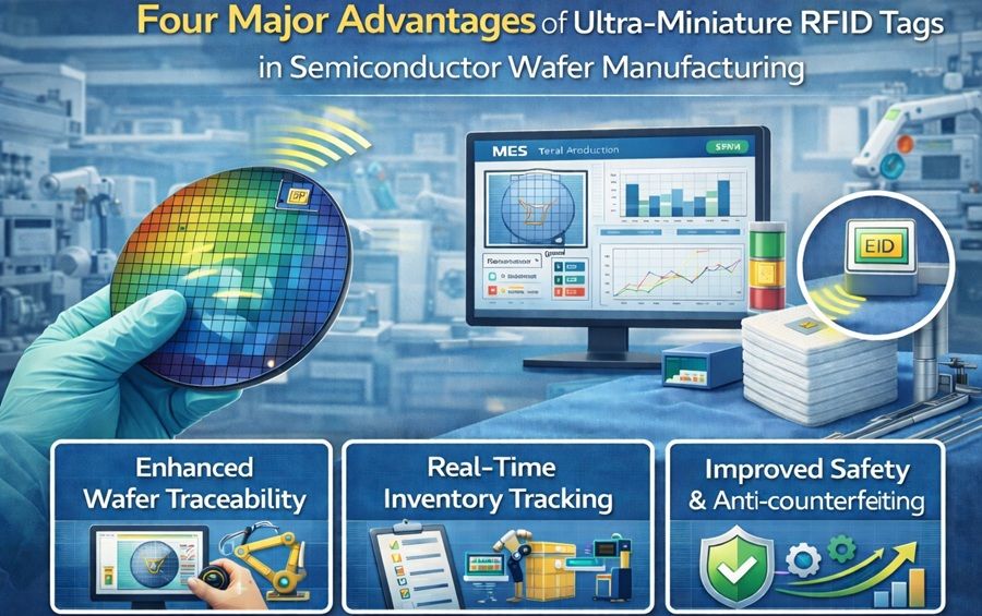
Four Core Advantages of Ultra-Small RFID Tags
1.Excellent Cleanroom Compatibility
Ultra-small RFID tags designed for semiconductor environments are encapsulated in inert materials such as ceramic or PEEK, meeting ultra-clean standards. For example, the customized tag solutions provided by RFIDHY have undergone rigorous outgassing testing of their encapsulation materials and adhesives, ensuring zero contamination in Class 1 cleanrooms. The tags can be seamlessly embedded within the FOUP or MTC (Mechanical Transfer Chuck) structure, without being exposed, fully adapting to the wafer fab’s CMP and wet cleaning processes.
2.Efficient Non-Line-of-Sight Reading Capability
Based on the UHF EPC Gen2 standard (such as ISO/IEC 18000-63), ultra-small RFID supports non-line-of-sight reading within a range of several meters. This means that fixed readers installed on AMHS tracks, stock, or load ports can automatically identify moving carriers in batches without requiring precise alignment. This significantly improves the automation level of material tracking, with read rates exceeding 99.99%, far surpassing the 85%-95% of barcodes.
3.Dynamic Data Rewriting and High Capacity
The built-in chip in each RFID tag (such as Impinj Monza R6 or Alien Higgs-9) provides over 512 bits of user memory and supports tens of thousands of data rewrites. This feature is crucial for wafer manufacturing:
- Real-time updating of wafer Lot ID, process steps, and measurement data
- Recording the usage cycle and maintenance history of carriers
- Enabling deep integration with MES (such as Promis or SPECFAB) and EAP systems
4.Unparalleled Durability and Long Lifespan
Semiconductor manufacturing environments involve extreme conditions, including high temperatures (heat treatment), corrosive chemicals, and high-energy radiation. Ultra-micro RFID tags offer significant durability advantages:
| Feature | Barcode Labels | Ultra-micro RFID Tags |
| Chemical Resistance | Poor, easily damaged by solvents | Excellent, resistant to acids, alkalis, and organic solvents |
| High Temperature Resistance | Usually below 150°C | Some models can withstand over 300°C (e.g., RFIDHY HT series) |
| Physical Wear | Surface printing is easily worn | Embedded packaging, scratch-resistant |
| Lifespan | Months, requiring frequent replacement | Up to 10 years or more, same lifespan as the carrier |
Enterprise Solutions: RFIDHY’s Deep Customization Services
The needs of semiconductor manufacturing are highly specialized. RFIDHY, with its deep customization capabilities, provides customers with end-to-end solutions from chip selection and antenna optimization to packaging design.
For example, for carriers that need to operate near EUV lithography areas, RFIDHY can provide low-metal content, radiation-resistant tag designs; for ultra-thin 300mm FOUPs, flexible tags with a thickness of less than 0.5mm can be developed to ensure that they do not affect the mechanical precision and Load Port docking of the carrier.
Q&A
1.Is integrating RFID into existing AMHS and MES systems very complex and costly?
Modern integration has been greatly simplified. RFID readers typically communicate with equipment via SECS/GEM or EAP protocols, with middleware handling data filtering and formatting, and interfacing with the MES system through standard APIs (such as REST).
Although the initial investment is higher than barcodes, considering the benefits in increased productivity, reduced errors, and lower labor costs, the total return on investment (ROI) is usually achieved within 12-18 months. One industry case study showed that the adoption of RFID reduced manual intervention in wafer WIP (work-in-progress) tracking by 70%.
2.Will RFID signals interfere with sensitive wafer manufacturing equipment?
No.
First, the UHF RFID operating frequency bands used in semiconductor manufacturing (such as the globally universal 865-868 MHz or 902-928 MHz) are certified industrial, scientific, and medical frequency bands.
Secondly, professional suppliers like RFIDHY conduct rigorous EMI (electromagnetic interference) testing before deployment to ensure that the reader’s transmission power and modulation methods fully comply with the requirements of sensitive equipment in the fab (such as metrology tools and inspection equipment). The tags themselves are passive devices, responding only momentarily during reading, with extremely low radiation.
3.How does RFID manage the cleaning and preventive maintenance (PM) cycles of wafer carriers (such as FOUPs)?
This is a typical application of the rewritable data advantage of RFID. Key data such as the last cleaning time, number of cleanings, last PM date, and access area permissions can be written to and updated on each carrier’s RFID tag.
When a carrier passes through a reader at a cleaning station or PM area, the system automatically updates the record and can trigger alerts (such as “This FOUP has reached its maximum usage limit”), enabling predictive maintenance and ensuring that the carrier’s condition always meets process cleanliness requirements—something that static barcodes cannot achieve.
Conclusion
In the process of moving towards smart manufacturing and Industry 4.0, the demand for data automation in semiconductor wafer manufacturing has far exceeded the capabilities of barcode technology. Ultra-small RFID tags, with their four core advantages of cleanroom compatibility, non-line-of-sight reading, rewritable data, and exceptional durability, not only solve tracking problems but also provide the data foundation for achieving fully automated fabs, precise traceability, and advanced analytics. Partnering with companies like RFIDHY, which possess deep industry knowledge and customization capabilities, is a strategic choice to ensure successful technology implementation, maximize investment value, and maintain a competitive edge.
Leave your contact detail now to get the latest price!